Determining the maximum operating frequency in Xilinx Vivado

How to determine the maximum operating frequency of the design? It is not straight forward in Vivado compared to ISE. Here is a step by step guide to do this.

Step 1: After finishing the code, run synthesis/implementation. Once it is completed, click on the ‘Constraints Wizard’ link on the SYNTHESIS tab of flow navigator. 

Capture

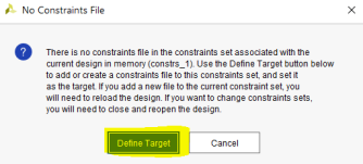
A ‘No Constraints File’ window will pop up asking to define the target first. Click on ‘Define Target’.

Capture

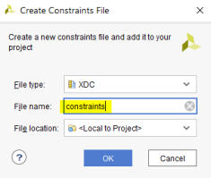
‘Define Constraints and Target window will be opened and click on ‘Create File’ if you don’t already have a constraints file.

Capture

Name the file and click OK

Capture

Select the created file and click OK

Capture

Step 2: Once the file is created, click again on the ‘Constraints Wizard’ option on the SYNTHESIS tab. A window will pop up asking for reloading the design. Click on ‘Reload’.

Capture

After reloading, click on the ‘Constraints Wizard’ option again. This time the following ‘Timing Constraints Wizard’ window will open. Click on next.

Capture.PNG

Next, the clock frequency needs to be defined. Provide the required frequency and click ‘Next’.

Capture

The other constraints can be defined if input delays need to be considered. Otherwise, uncheck all the other constraints and click ‘Finish’ at the end.

Capture.PNG

Before clicking ‘Finish’, make sure you have checked the boxes for the reports you are needed.

Capture

Step 3: After finishing, run implementation and that will show the WNS (Worst Negative Slack) in the project summary.

Capture.PNG

Slack is calculated as ‘required time – arrival time’.  WNS shows the spare time we have after meeting the timing requirements. So WNS=6.44ns means it takes only 3.56ns (10ns-6.44ns, where 10ns is the time period for 1 clock cycle for a frequency of 100MHz which we were provided in the constraints file) to complete the execution. To Find the maximum frequency, we have to edit the constraints file for different frequencies until the least possible WNS value we can get which is not negative. Now we checked for operating frequency for 100MHz, and we see that it requires only 3.56 ns for execution.

We can now add a frequency of 300MHz in the constraints file and see what is the WNS. If the WNS is still greater than zero, we can increase the frequency, until no more increment can be done. For example, you set 400MHz in the constraints file and you get a WNS = 0.01ns. When you increase the frequency to 401MHz, the WNS goes negative. That means your maximum operating frequency is 400MHz.

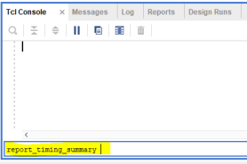
If you need to see an elaborated timing report, just type the tcl command ‘report_timing_summary’ on tcl console and press ‘Enter’.

Capture

This will give you an elaborated timing summary with all the clock details.

Dual Port RAM (Block RAM)

The common understanding is that clocked RAM is always inferred as block RAM. This is not really true. The way it chooses between Block RAM and LUTRAM depends on the design methodology also.

Let’s see a clocked dual port RAM which will be inferred as Block RAM (BRAM)

A dual port RAM as LUTRAM is given in Dual port RAM (clocked LUTRAM)

Code:


module single_port_ram#(
parameter ADDR_WIDTH = 10,
parameter DATA_WIDTH = 16,
parameter DEPTH = 1<<ADDR_WIDTH)
(
input clk,
input [ADDR_WIDTH-1:0] addr_0, addr_1,
input wr_en_0, wr_en_1,oe_0, oe_1,
input [DATA_WIDTH-1:0] data_in_0, data_in_1,
output reg [DATA_WIDTH-1:0] data_out_0,data_out_1
);

reg [DATA_WIDTH-1:0] memory_array [0:DEPTH-1];

always @ (negedge clk)
begin
if(wr_en_0 && !wr_en_1 && !oe_0) begin
memory_array[addr_0] <= data_in_0;
data_out_0 <= 0;
end
else if(!wr_en_0 && oe_0)begin
data_out_0 <= memory_array[addr_0];
end
else
data_out_0 <= 0;
end

always @(negedge clk)begin
if(wr_en_1 && !wr_en_0 && !oe_1) begin
memory_array[addr_1] <= data_in_1;
data_out_1 <= 0;
end
else if(!wr_en_1 && oe_1)begin
data_out_1 <= memory_array[addr_1];
end
else
data_out_1 <= 0;
end

endmodule
 

Resource Utilization:

 
res

Dual port RAM (clocked LUTRAM)

The common understanding is that clocked RAM is always inferred as block RAM. This is not really true. The way it chooses between Block RAM and LUTRAM depends on the design methodology also.

Let’s see a clocked dual port RAM which will be inferred as LUTRAM.

A dual port RAM as block RAM is given in Dual Port RAM (Block RAM)

Code:


module dualport_lutram#(
parameter ADDR_WIDTH = 10,
parameter DATA_WIDTH = 16,
parameter DEPTH = 1<<ADDR_WIDTH
)
(
input clk, wr_en_0,wr_en_1,oe_0,oe_1,
input [ADDR_WIDTH-1:0]addr_0, addr_1,
input [DATA_WIDTH-1:0] din_0,din_1,
output reg [DATA_WIDTH-1:0] dout_0, dout_1
);


reg [DATA_WIDTH-1:0] memory [0:DEPTH-1];

always@(negedge clk)begin
if(wr_en_0 && !oe_0)
memory[addr_0] <= din_0;
else if(wr_en_1 && !oe_1)
memory[addr_1] <= din_1;

end

always@(negedge clk)begin
if(!wr_en_0 && oe_0)
dout_0 <= memory[addr_0];
else
dout_0 <= 0;
if(!wr_en_1 && oe_1)
dout_1 <= memory[addr_1];
else
dout_1 <= 0;
end

endmodule

Resource Utilization:

res

We can see that instead of BRAM, LUTRAM is inferred.

Full adder using two half adders

A full adder using two half adders is implemented here.

The equation for the sum and carry are:

Sum = A xor B xor Cin
Carry = (A xor B).Cin + A.B

fa

Code:


module full_adder(
input a,b,cin,
output sum, carry
);

wire temp_sum, temp_carry_1,temp_carry_2;
half_adder HA1(.a(a),.b(b),.sum(temp_sum),.carry(temp_carry_1));
half_adder HA2(.a(temp_sum),.b(cin),.sum(sum),.carry(temp_carry_2));
assign carry=temp_carry_1|temp_carry_2;


endmodule

module half_adder(
input a,b,
output reg sum,carry
);
always@(*)begin
{carry,sum} = a+b;
end
endmodule

Half adder (Using gates and behavioural code)

Let’s see how we can implement synchronous half adder using gates and also by using behavioural modelling.

Using Gates:


module half_adder_using_gates(
input clk,
input a,b,
output reg sum,carry
);


always@(posedge clk)begin
sum <= a^b;
carry <= a&b;
end


endmodule

Behavioural modelling:


module half_adder(
input clk,
input a,b,
output reg sum,carry
);


always@(posedge clk)begin
{carry,sum} = a+b;
end

endmodule

Block Ram ( Single port)

When you need larger blocks of memory for your design, it is better to go for block RAM instead of distributed RAM. Distributed RAM is best suitable for small chunks of data storage which uses LUTs for memory implementation. Blocks RAMs are faster too compared to distributed RAM. Block RAM is synchronous and requires a clock.

A simple code for Block RAM is given here.


module bram #(
parameter ADDR_WIDTH = 8,
parameter DATA_WIDTH = 8,
parameter DEPTH = 256)
(
input clk,
input [ADDR_WIDTH-1:0] addr,
input wr_en,
input [DATA_WIDTH-1:0] data_in,
output reg [DATA_WIDTH-1:0] data_out
);


reg [DATA_WIDTH-1:0] memory_array [0:DEPTH-1];


always @ (posedge clk)
begin
if(wr_en) begin
memory_array[addr] <= data_in;
end
else begin
data_out <= memory_array[addr];
end
end
endmodule

Shift Operators

If you are fond of behavioural modelling, then shift operators will help you to create a shift register in an easy way. Also, Right shifting is actually divided by 2 operation and left shifting is multiply by 2. But the beginners might get confused with the logical and arithmetic shift operators.

‘<<‘  – logical shift left

‘>>’ – logical shift right

‘<<<‘ – arithmetic shift left

‘>>>’ – arithmetic shift right

Logical shift operators simply shift the numbers left or right and the vacant positions after shifting are filled with zeros.

for example:

01010110 >> 1 = 00101011 (The red coloured bit (LSB) will be omitted and green coloured bit replaces it (MSB)).

01010110 >> 3 = 00001010

01010110 << 1 = 10101100 

01010110 << 3 = 10110000

Arithmetic shift operators shift numbers left or right same as logical operators but, the MSB remains the same for the right shift operation.  In other words, arithmetic shift operators are best suited for signed numbers.

For right shift, the vacant positions are filled with either ‘1’ or ‘0’ depending on the MSB, and for left shift, the vacant positions are filled with ‘0’.

01010110 >>> 1 = 00101011

11010110 >>> 1 = 11101011

01010110 >>> 3 = 00001010

11010110 >>> 3 = 11111010

01010110 <<< 1 = 10101100 

01010110 <<< 3 = 10110000

11000110 <<< 3 = 00110000


Binary Multiplier using Vedic Mathematics (Urdhva-Tiryagbhyam method)

Multiplication operations are complex for a hardware designer. So, optimisations in multipliers are always a good thing to do when we design hardware. Vedic mathematics methods are very efficient in terms of area and delay for hardware design. A simple 4×4 multiplier using Urdhva-Tiryagbhyam method is presented here. But, note that this method is efficient only when the bitwidth of the operand is less than 8-bit.

Line notation of Urdhva-Tiryagbhyam:

ut

Calculation:


calccalc1calc2

Reference


module UT_4x4_mul(
a,b, //4-bit inputs
product, //8-bit output
clk
);
input clk;
input [3:0] a,b;
output reg [7:0] product;
reg G00,G01,G10,G11,G02,G20,G30,G21,G12,G03;//AND gates
reg G31,G22,G13,G32,G23,G33;

half_adder A1_HA(.a(G10),.b(G01),.sum(p1),.cy(c1),.clk(clk));
adder_4_to_2 A2_A42(.a(c1),.b(G20),.d(G11),.cin(G02),.sum(p2),.cout(c2),.clk(clk));
adder_5_to_2 A3_A52(.a(c2),.b(G30),.d(G21),.e(G12),.cin(G03),.sum(p3),.cout(c3),.clk(clk));
adder_4_to_2 A4_A42(.a(c3),.b(G31),.d(G22),.cin(G13),.sum(p4),.cout(c4),.clk(clk));
full_adder A5_FA(.a(c4),.b(G23),.cin(G32),.sum(p5),.cout(c5),.clk(clk));
half_adder A6_HA2(.a(c5),.b(G33),.sum(p6),.cy(c6),.clk(clk));

always@(posedge clk)
begin

G00<=a[0]&&b[0];
G01<=a[0]&&b[1];
G10<=a[1]&&b[0];
G11<=a[1]&&b[1];
G02<=a[0]&&b[2];
G20<=a[2]&&b[0];
G30<=a[3]&&b[0];
G21<=a[2]&&b[1];
G12<=a[1]&&b[2];
G03<=a[0]&&b[3];
G31<=a[3]&&b[1];
G22<=a[2]&&b[2];
G13<=a[1]&&b[3];
G32<=a[3]&&b[2];
G23<=a[2]&&b[3];
G33<=a[3]&&b[3];

product={c6,p6,p5,p4,p3,p2,p1,G00};
end
endmodule

module half_adder(a,b,sum,cy,clk);
input a,b;
input clk;
output reg sum,cy;
always@(posedge clk)
begin
{cy,sum}=a+b;
end
endmodule

module full_adder(a,b,cin,sum,cout,clk);
input a,b,cin;
input clk;
output reg sum,cout;
always@(posedge clk)
begin
{cout,sum}=a+b+cin;
end
endmodule

module adder_4_to_2(a,b,d,cin,sum,cout,clk);
input a,b,d,cin;
input clk;
output reg sum,cout;
always@(posedge clk)
begin
{cout,sum}=a+b+d+cin;
end
endmodule

module adder_5_to_2(a,b,d,e,cin,sum,cout,clk);
input a,b,d,e,cin;
input clk;
output reg sum,cout;
always@(posedge clk)
begin
{cout,sum}=a+b+d+e+cin;
end
endmodule

Custom floating point adder

A floating point adder which uses custom mantissa and exponent sizes is presented here. Mantissa size:4, exponent size:6. For a floating point adder, a leading edge detector is required after mantissa addition. Though, since only 3 bits need to be checked, we can use a Mux instead (if loop) in this case.


module FP_add(
input clk, in_ready,
input [10:0] a,b,
output reg [10:0] sum,
output reg done
);
wire sign_a,sign_b;
reg sign_sum,big_sign,small_sign;
wire [5:0] exp_a,exp_b;
reg [5:0] exp_sum,big_exp;
wire [3:0] man_a,man_b;
reg [3:0] man_sum,big_mant, small_mant;
reg [4:0] temp_man_big,temp_man_small;
reg [5:0] temp_man_sum;
reg [5:0] exp_diff;

assign {sign_a,exp_a,man_a}=a;
assign {sign_b,exp_b,man_b}=b;

always@(posedge clk)begin
if(a==0 && b==0)begin
sum=0;
done=1'b1;
end
else if(a==0 && b!=0)begin
sum=b;
done=1'b1;
end
else if(a!=0 && b==0)begin
sum=a;
done=1'b1;
end
else begin
if(in_ready)begin
if(exp_a>exp_b)begin
big_exp=exp_a;
big_sign=sign_a;
small_sign=sign_b;
big_mant=man_a;
small_mant=man_b;
exp_diff=exp_a-exp_b;
end
else if (exp_a==exp_b)begin
if(man_a>man_b)begin
big_exp=exp_a;
big_sign=sign_a;
small_sign=sign_b;
big_mant=man_a;
small_mant=man_b;
exp_diff=exp_a-exp_b;
end
else begin
big_exp=exp_b;
big_sign=sign_b;
small_sign=sign_a;
big_mant=man_b;
small_mant=man_a;
exp_diff=exp_b-exp_a;
end
end
else begin
big_exp=exp_b;
big_sign=sign_b;
small_sign=sign_a;
big_mant=man_b;
small_mant=man_a;
exp_diff=exp_b-exp_a;
end
temp_man_big={1'b1,big_mant};
temp_man_small={1'b1,small_mant}>>exp_diff;
if(big_sign==small_sign)begin
temp_man_sum=temp_man_big+temp_man_small;
end
else if(big_sign!=small_sign)begin
temp_man_sum=temp_man_big-temp_man_small;
end
if(temp_man_sum[5]) begin
man_sum=temp_man_sum[4:1];
exp_sum=big_exp;
sign_sum=big_sign;
sum={sign_sum,exp_sum,man_sum};
done=1'b1;
end
else if(temp_man_sum[4])begin
man_sum=temp_man_sum[3:0];
exp_sum=big_exp;
sign_sum=big_sign;
sum={sign_sum,exp_sum,man_sum};
done=1'b1;
end
else if(temp_man_sum[3])begin
man_sum={temp_man_sum[2:0],1'b0};
exp_sum=big_exp-1'b1;
sign_sum=big_sign;
sum={sign_sum,exp_sum,man_sum};
done=1'b1;
end
else if(temp_man_sum[2])begin
man_sum={temp_man_sum[1:0],2'b0};
exp_sum=big_exp-2'b10;
sign_sum=big_sign;
sum={sign_sum,exp_sum,man_sum};
done=1'b1;
end
end
end
end
endmodule

Custom floating point multiplier

A simplified custom floating point multiplier is presented here. When we design with platforms having low resources, using a full-fledged floating point multiplier would take too much of the resources available. One solution is to design a custom floating point multiplier with a custom exponent and mantissa size. Such a multiplier with 6 bit exponent and 4 bit mantissa is presented here. Note that no rounding scheme is used here. Many different rounding schemes are present and if you want to employ one, the logic can be applied just before the product mantissa calculation after mantissa multiplication.


module FP_mul_6_4(
input clk,in_ready,
input [10:0] a,b,
output reg [10:0]product,
output reg done
);

reg sign_a,sign_b,sign_p;
reg [5:0] exp_a,exp_b,exp_p;
reg [3:0] man_a,man_b,man_p;
reg [5:0] temp_expa,temp_expb,temp_expp;
reg [4:0] temp_mana,temp_manb;
reg [9:0]temp_manp;

always@(posedge clk) begin
if(a==0||b==0)begin
product=0;
done=1'b1;
end
else begin
if(in_ready)begin
{sign_a,exp_a,man_a}<=a;
{sign_b,exp_b,man_b}<=b;
temp_mana={1'b1,man_a};
temp_manb={1'b1,man_b};
temp_expa=exp_a-6'd31;
temp_expb=exp_b-6'd31;

sign_p=sign_a^sign_b;
temp_expp = temp_expa+temp_expb;
temp_manp = temp_mana*temp_manb;
if(temp_manp[9]) begin
man_p=temp_manp[8:5];
exp_p=temp_expp+6'd32;
product={sign_p,exp_p,man_p};
done=1'b1;
end
else if(temp_manp[9]==0)begin
man_p=temp_manp[7:4];
exp_p=temp_expp+6'd31;
product={sign_p,exp_p,man_p};
done=1'b1;
end
end
end
end
endmodule